Mr. zptouch01
Leave a message Mr. zptouch01
Mr. zptouch01
Leave a messageInspection of appearance
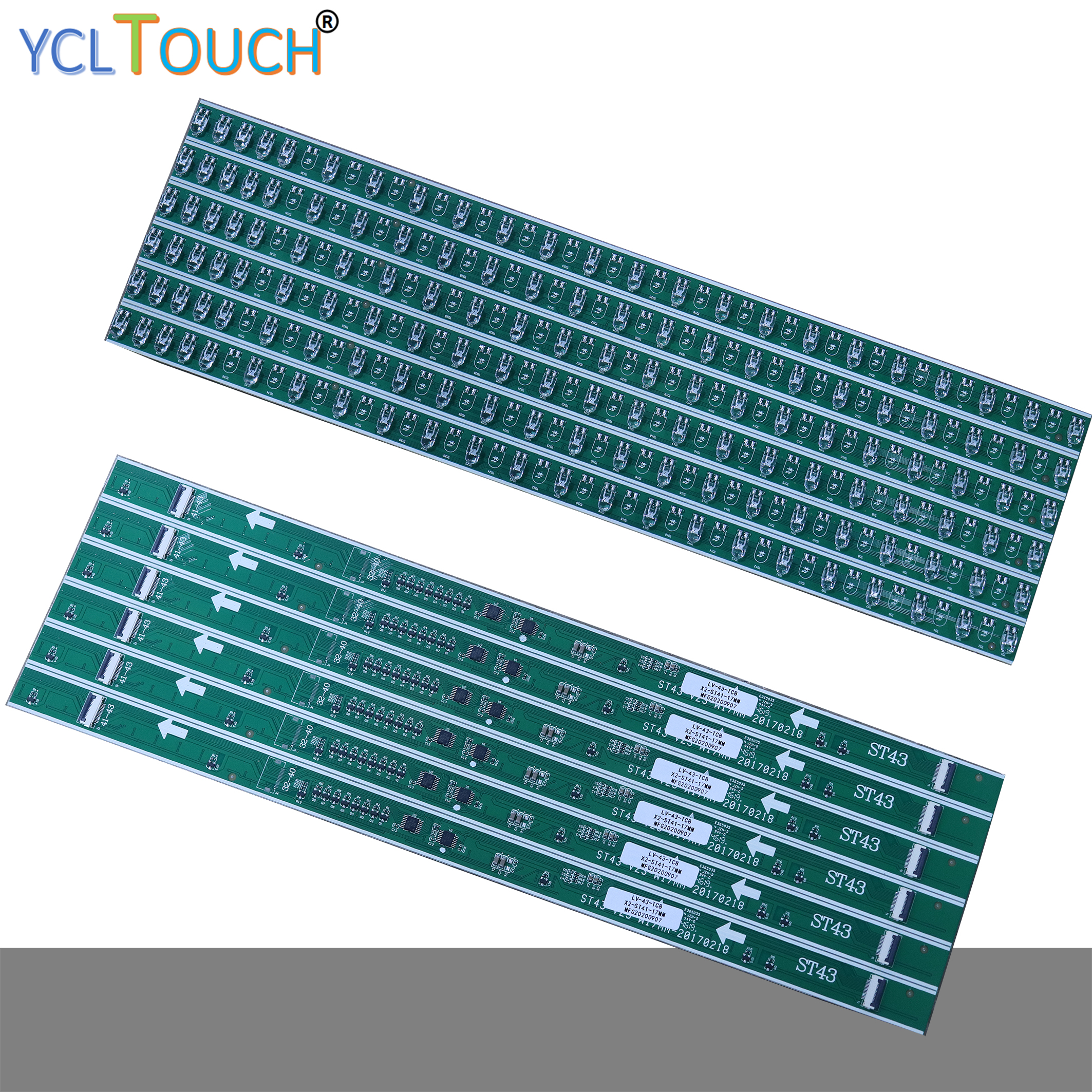
Direct visual inspection of the appearance of infrared PCBA, check whether the components are missing or damaged, whether the pins are regular, and whether the solder connection is normal, so as to preliminarily troubleshoot obvious physical defects and some bad welding problems. For example, check whether the patch capacitor is broken, discoloring and other abnormalities, whether the plug-in element is firmly installed and perpendicular to the plate, for surface mounted chips, pay attention to the fit of the pin and the pad, whether there are signs of virtual welding caused by the pin is not completely saturated with solder, and whether there is a short circuit bridge between adjacent pads caused by excessive tin.
Electrical connectivity test
With the help of professional equipment, the signal is applied to the PCB line to detect the on-off status between the lines, accurately locate the open or short circuit position, and ensure the basic conduction of the electrical line. The test usually uses high-precision resistance measuring instrument, current and voltage detector and other professional tools. First, the specific electrical signal is input at the starting test point of the circuit board, and then the signal feedback of each node is gradually detected along the line. For example, in multi-layer circuit boards, signals need to traverse different inter-layer lines. Through the segmented detection of each layer line, open circuit problems caused by poor lamination process or line etching defects can be effectively found, as well as short circuit risks caused by unreasonable circuit design or welding errors, so as to ensure the integrity and reliability of the entire electrical network.
Functional verification test
It simulates the input signal of the actual working scene of PCBA, and checks whether the output of its functions meets the design expectations, so as to judge the integrity and accuracy of the whole PCBA function.
Automatic optic inspection (AOI)
The optical equipment is used to scan the surface of PCBA, and the surface defects such as welding defects and component offset are detected quickly and efficiently by comparing the image processing with the standard image.

Automatic X-ray inspection
The X-ray penetration characteristics are used to generate the internal image of PCBA, which can effectively find the hidden welding problems inside the multilayer board, such as the quality of the solder joint of the BGA package.
Flying probe
Flexible electrical performance testing through movable probe contact test point without special fixture, suitable for small batch or prototype PCBA testing.
Aging test
The PCBA is placed in an aging box that simulates the working environment for a long time to expose potential quality risks in advance and ensure its stability and reliability in long-term use.
Previous: What is PCBA failure?

Privacy statement: Your privacy is very important to Us. Our company promises not to disclose your personal information to any external company with out your explicit permission.

Fill in more information so that we can get in touch with you faster
Privacy statement: Your privacy is very important to Us. Our company promises not to disclose your personal information to any external company with out your explicit permission.